- 讲解应用于微波集成电路的高电子迁移率晶体管(HEMT)和异质结双极晶体管(HBT)的工作原理;
- 计算器件和/或子电路之间的失配并设计匹配网络;
- 描述并绘制单片微波集成电路(MMIC)的工艺流程;
- 应用行业标准微波电路仿真工具来预测无源和有源微波器件和电路的响应;
- 使用参数设计无源和有源微波集成电路元件,例如滤波器、放大器、振荡器和低噪声接收器。
考点整理
无损传输线
在无损情形下有,
有耗媒质的复传播常数公式
指向原始笔记的链接
为衰减常数; 为相位常数。
以上公式可以理解为,
特征阻抗也可以简化为,
波长为,
相速度为,
无耗传输线上电压和电流的一般解可以写为,
反射系数与回波损耗
反射系数定义如下,
反射系数定义式
指向原始笔记的链接
是反射系数; 是反射电压; 是入射电压; 为传输线的特征阻抗,通常为 ; 为电路的负载阻抗值。
回波损耗定义如下,
回波损耗定义式
指向原始笔记的链接
为回波损耗,单位为 ; 为输入功率; 为反射功率; 为反射系数。
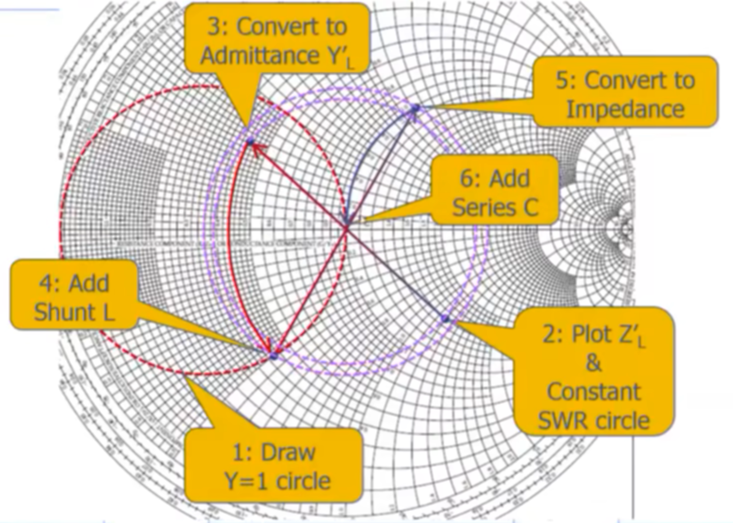
使用仅含阻抗圆的史密斯圆图进行阻抗匹配
使用仅含阻抗圆的史密斯圆图进行阻抗匹配
相较于复合史密斯圆图而言步骤较为复杂,涉及了阻抗和导纳在史密斯圆图上的转换。
阻抗和导纳在史密斯圆图上的转换
- 画出阻抗点;
- 以阻抗点到匹配点为半径,以匹配点为圆心作圆;
- 画出通过阻抗点的直径,相交于另一半圆的点即为对应的导纳点;
- 按照仅含阻抗圆的史密斯圆图读出的「阻抗值」即为导纳值。
阻抗匹配
按照上图步骤进行即可。
[! attention] 注意一点,在将阻抗转换为导纳之后,串并联电感和电容的方向与原本的方向相反,电感往下,电容往上。
Transclude of 史密斯圆图#^715877随后计算阻抗值即可。需要注意阻抗-导纳值的转换以及乘上系统阻抗值。
电感阻抗计算式
指向原始笔记的链接 指向原始笔记的链接电容阻抗计算式
指向原始笔记的链接

微带线和波导
优缺点比较
| 方面 | 微带线 | 波导 |
|---|---|---|
| 优点 | 体积小、重量轻、使用频带宽、可靠性高和制造成本低 | 功率容量大、损耗低, 对基底变化不敏感 |
| 缺点 | 损耗稍大,功率容量小; 对基底的变化敏感; | 体积大、重量大,不利于集成 |
阻抗计算
微带线特征阻抗计算式(影响参数)
Transclude of 微波集成电路-Slides-总结-1.0#微带线特征阻抗计算
共面波导特征阻抗计算(影响参数)
共面波导阻抗计算
指向原始笔记的链接共面波导阻抗计算方法
CPW 中的场以及电磁能量几乎在空气和电介质之间平均分配,尤其是当间隙相对于电介质厚度较小时。在计算 CPW 特性阻抗时需要先计算以下两个参数。
CPW 的有效相对介电常数及其中央条带相对占比参数
。 CPW 的有效相对介电常数
指向原始笔记的链接
为基材的相对介电常数。 对于 h/s ≥1,精确度为 1.5%。而参数
则是由以下公式进行计算。 CPW 的有效相对介电常数参数 k 计算式
指向原始笔记的链接
为中央条带的的宽度; 为中央条带两旁的空气的宽度。 通常来说我们会使用简化的 CPW 的相对介电常数计算式。由此可以得出 CPW 的特性阻抗为,
CPW 特性阻抗计算式
指向原始笔记的链接
为椭圆积分, , ,计算其比例 较简单; 为 CPW 的相对介电常数。 指向原始笔记的链接CPW 特性阻抗计算式中椭圆积分比例计算式
指向原始笔记的链接
滤波器设计
低通原型设计
记住低通原型设计的前提是,
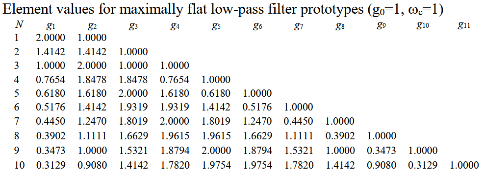
最平坦低通滤波器设计
对于归一化低通设计,其源阻抗是
,其截止频率为 ,并且 。由此构建的 N 阶梯形电路的元件值已经被制作成表格。
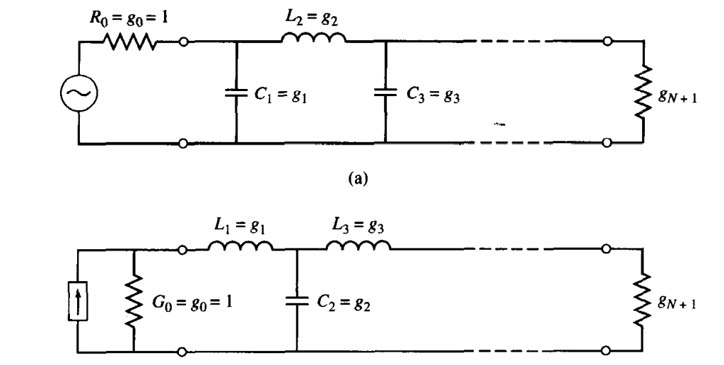
1. 电路选择
对于一个最平坦响应的低通滤波器,我们可以使用以下两种通用电路:
从信号源开始,我们可以选择第一个元器件为并联还是串联,之后的元件串并交替,两个电路均能够实现相应的功能。
第一个电抗性元件为电容的称为
(pi)型电路,第一个电抗性元件为电感的被称为 (tee)型电路。 Question
串并联之间有什么区别吗,会影响什么性能呢? 答:无区别,互为对偶,两者给出同样的响应。
对于有
个电抗性元件的滤波器,这些元件值已编号为从源阻抗 到负载阻抗 。这些元件在串联和并联之间交替出现,且 有下面的定义: 于是,上图所示的两种电路就可以认为是互为对偶的,两者给出同样的响应。
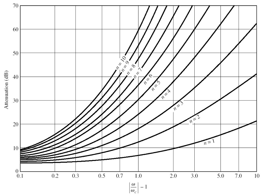
2. 阶数确定
给定固定频率时的插入损耗值,我们可以根据下表确定滤波器的阶数:
一般题目会给出要求,例如“在 2GHz 时插入损耗至少为30dB”,题干中又给出截止频率为 1GHz,这里
指向原始笔记的链接,再减去 1 之后就等于 1。如果想达到 的衰减,按照曲线而言则至少需要 5 阶。5 阶就意味着需要 5 个集总元件。
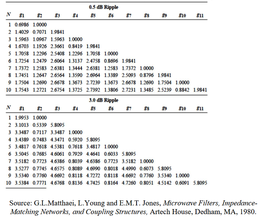
等纹波低通滤波器设计
对于归一化低通设计,其源阻抗是
,其截止频率为 ,并且 。由此构建的 N 阶梯形电路的元件值已经被制作成表格。 [! attention] 注意,负载阻抗对于偶数
有 。 等纹波滤波器一般分为两种:带内纹波为 3dB 和带内纹波为 0.5dB。
电路结构
电路基本结构和 最平坦低通滤波器原型设计 是一样的。
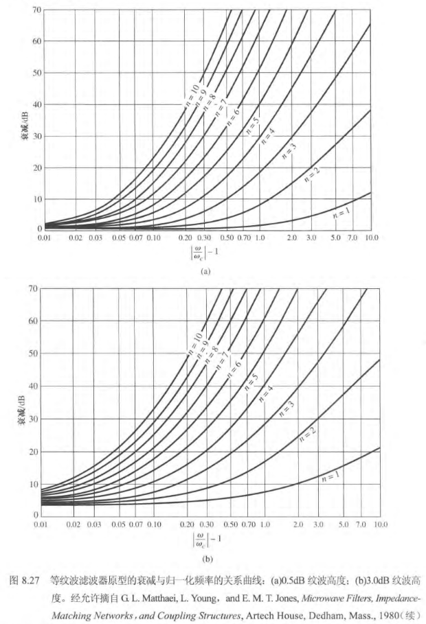
确定滤波器阶数
通过下图,我们可以知道多少阶的滤波器可以满足我们的需求。
确定阶数之后,即可在「等纹波低通滤波器原型的元件值」表中查找原型器件值。
指向原始笔记的链接

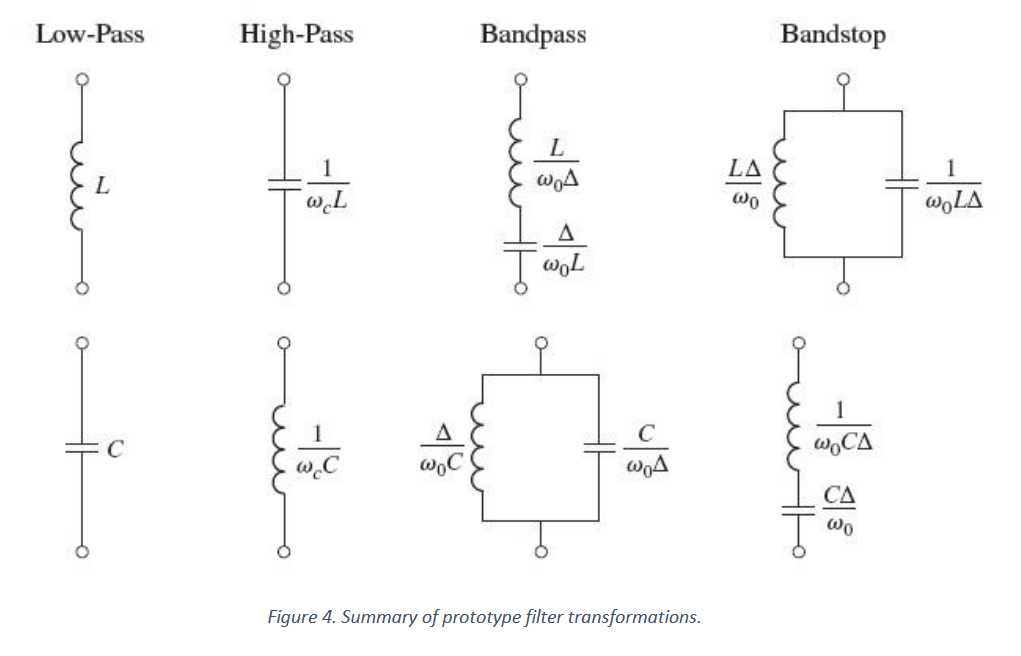
带通转换
频率缩放公式
Transclude of 微波集成电路-Slides-总结-1.0#低通到带通
阻抗缩放
串联电感
并联电容
原型滤波器元件转换
放大器
最大转换功率增益
首先我们需要给出假设:It is always assumed that the measurements are taken with a
然后计算
Rollet 条件及其辅助条件
无条件稳定的Rollet 条件为,
辅助条件为,
当不满足的时候,为潜在不稳定状态
指向原始笔记的链接
随着,一般题目会给出条件
如果无法单边近似
如果无法进行单边近似,那么就相当于在使用双边晶体管(
如果不是,则需要导出稳定性圆,并且需要将史密斯圆图内的圆上的点同时与源和负载稳定性圆相匹配。
硬件实现流程
由于它是单边的,因此物理实现变得更加容易。这意味着我们可以为源设计一个独立于负载的短路匹配电路。这可以通过共轭匹配 S11 和 S22 来实现(注:学生可能会提到,使用微波 CAD 软件包,只需调整每个匹配元件即可,非常简单)。
趋肤深度
计算公式以及 10 GHz 下的经验公式
趋肤深度计算式
指向原始笔记的链接
为导体的电阻率; 为角频率; 为频率; 为相对磁导率; 为真空磁导率; 为电导率;
真空磁导率数值
Transclude of 真空磁导率常数
在计算趋肤深度的时候用来近似。
Power Amplifiers and MMICs
1. What is meant by the term Monolithic when considering microwave integrated circuits.
The word monolithic describes the fundamental property of a MMIC, in that is formed from a single piece of semiconductor material.
2. Discuss the relative advantages and disadvantages of silicon (Si) and Gallium Arsenide (GaAs) as substrate materials for Monolithic Microwave Integrated Circuits.
GaAs has traditionally been used as the substate material in MMICs due to its high electron mobility, which allows it to operate at higher speeds. In addition, because it has a higher band gap it is also a semi-insulating substrate material.
Silicon on the other hand is more abundant and with the advancement of silicon germanium transistors is now commonly used at microwave frequencies.
Nevertheless, GaAs is able to operate well into the millimetre wave spectrum.
3. Why is the dominance of GaAs at microwave frequencies is now being challenged because of silicon germanium (SiGe) technology.
Whilst GaAs has significant material advantages over Si, the abundance and low cost of Si means that it would be beneficial if it could be used as a substrate material. Another motivation for using Si as a MMIC is that it can be integrated with analog, RF and digital functions on a single integrated circuit. To enable this a material is needed that can be epitaxially grown on a Si substrate. This is possible with SiGe. The SiGe epitaxial layer provides high electron mobility in transistors that are equivalent or better than GaAs. SiGe can be used in the fabrication of HBT and HEMTS.
4. Discuss what limits the frequency of use of SiGe transistors.
The silicon substrate (~20 GHz)
5. Summarize the nine wafer processing steps
- Crystal Growth
- Wafer Slicing
- Surface Polishing
- Photolithography
- Etching
- Doping
- Thin Film Deposition
- Annealing
- Device Packaging
6. Discuss the design issues faced when via holes are used with microstrip shunt components.
- through-hole and microstrip shunt components can affect the impedance of input and output ports
- integration into a package may add complexity to the design
- may take up more space and may require denser wiring
7. Discuss the effect of reducing the thickness of the substrate on the thermal management of a MMIC power amplifier.
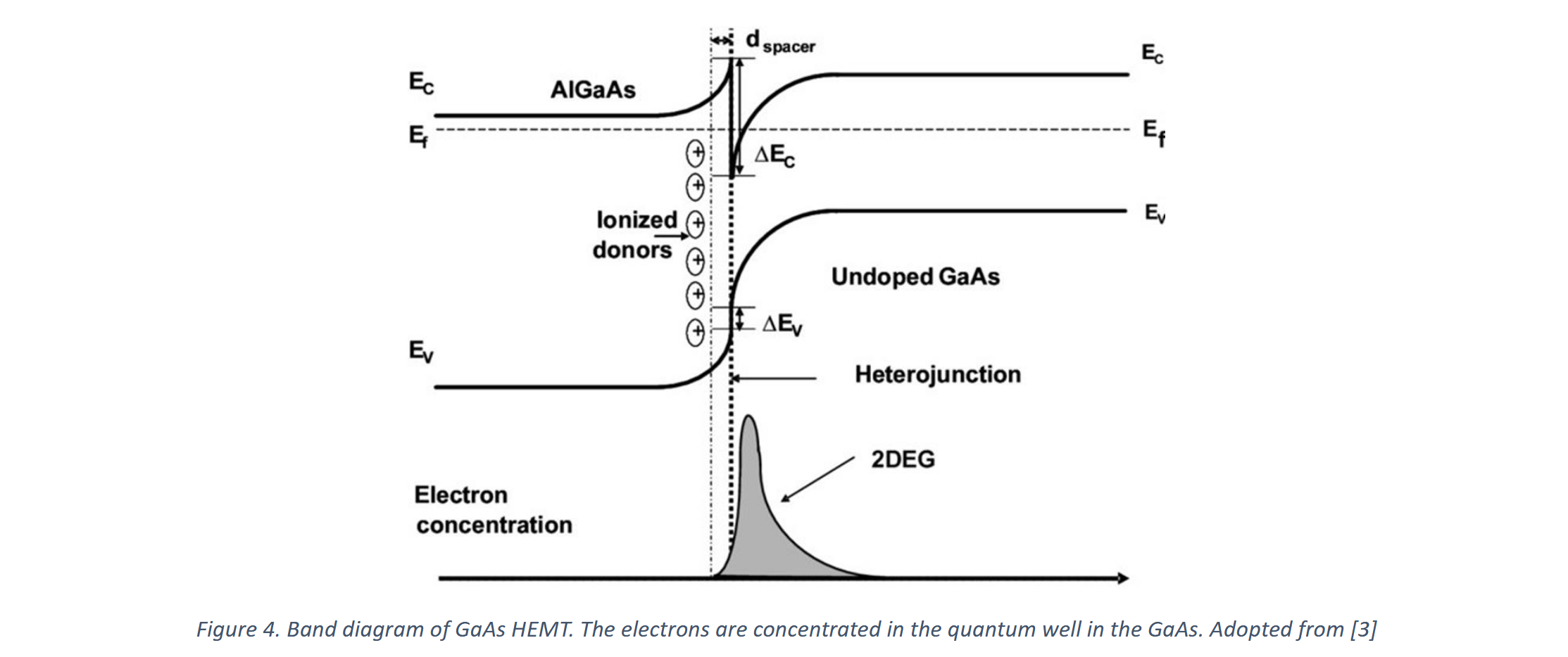
8. Describe the structure of a High Electron Mobility Transistor.
A high-electron-mobility transistor (HEMT), is a field effect transistor that incorporates a junction between two materials of different band gaps. This is termed a heterojunction (and this forms the conducting channel instead of a doped region). A commonly used material combination for the heterojunction is GaAs with AlGaAs.
In HEMTs high mobility electrons are generated using the heterojunction of a highly doped wide-bandgap n-type AlGaAs and an undoped narrow-bandgap channel layer with no dopantimpurities, GaAs. The electrons generated in the thin n doped AlGaAs layer drop completely into the GaAs layer, which forms a depleted AlGaAs layer.
This is due to the heterojunction created by different band-gap materials forming a quantum well (or valley) within the conduction band of the GaAs. They are confined within this valley and form what is termed a 2-dimensional electron gas (2-DEG).
The electrons avoid colliding with any impurities because the GaAs layer is undoped. The effect of this is to create a very thin layer of highly mobile electrons, of very high concentration. The high mobility of the electrons and the lack of collisions means they can be used to make transistors with high operating frequencies and low noise figure.

9. Explain how a 2-dimensional electron gas (2-DEG) is formed in a HEMT, and how this is useful when considering microwave transistors.
Need to draw a Band diagram.
10. On a MMIC transmission lines are usually microstrip and coplanar waveguide (CPW). Briefly describe the parameters that determine their line impedance.

Microstrip: Line width and dielectric permittivity and thickness.
CPW: Line width, ground plane spacing, substrate permittivity and thickness.
11. describe the five chip-rejection reasons
The chip-rejection reasons are generally brokendown into the following areas: processing yield, dc and RF test yield, saw and dicing yield, visual yield, and packaging yield。
12. Benefits and Disadvantages of MMICs
Benefits
- Component density is higher. Thousands of devices can be fabricated in a single MMIC simultaneously during fabrication with relative ease.
- Due to the higher component density the cost of fabrication is lower.
- There are minimal mismatches between components on the MMIC.
- The signal delay is minimised due to shorter distances being possible between components on a MMIC.
Disadvantages
- Overall performance of MMIC is compromised as the material for each element is restricted by the substrate and, hence, optimal materials cannot be used for each element individually.
- Power handling capacity is reduced due to proper heat transfer materials not being used in the fabrication of MMIC.
- “Trimming” adjustments are impossible. Hence, troubleshooting or reworking is impossible.
- It is prohibitively expensive to fabricate small quantities of MMICs.
13. Discuss the problem that arises from this high gain when HEMT is under lower microwave frequencies.
It is important to consider the stability at all frequencies. For example, a MMIC (Monolithic Microwave Integrated Circuit) low noise amplifier would typically use a HEMT as it would achieve high gain and low noise at microwave and millimetre wave frequencies. The device maybe stable at the design frequency but they will have very high gain at MHz and low-GHz frequencies and the designed amplifier is then likely to be unstable at these wavelengths. `