Non-Planar Metallization
![[Pasted image 20250425214050.png#pic_75center|]]
- Surface non-planarity in an IC is cumulative, starting from the original flat Si wafer.
- It is caused by both non-uniform film thickness across the wafer and the patterned topology of IC features such as gates or wiring.
- 集成电路(IC)中的表面不平坦性是累积性的,起始于原始的平坦硅片。
- 其形成原因包括晶圆上膜层厚度的不均匀性,以及诸如栅极或布线等IC特征的图案化拓扑结构。
Relative Surface Topology of Multilevel Metallization without Planarization
![[Pasted image 20250425214322.png#pic_50center|]]
- Upper metal layers for power supply and ground busses must have increased thickness for carrying higher current whereas low current signal busses are placed in the lower level metal layers. 用于电源和接地汇流排的上层金属层必须增加厚度,以承载更高的电流,而低电流信号汇流排则放置在较低层的金属层中
- This non-planar topology makes both etching and uniform filling of all vias in the inter-metal dielectric more difficult. Finally, at some level of non-planarity, both via etching and via filling become impossible to achieve with high yield.
- 这种非平坦拓扑结构使得金属间介电层中的所有通孔的蚀刻和均匀填充更加困难。最终,在某个非平坦度水平下,通孔的蚀刻和填充将难以实现高良率
Problems Arising From Non-Planar Topography
![[Pasted image 20250425214559.png#pic_75center|]]
- Photolithography Issues:
- Depth of Focus (DOF)
- Light reflection at steps causing notching 阶梯结构处的光反射导致刻蚀缺陷
- Resist thickness variation over steps 阶梯结构上的光刻胶厚度变化
- CMP enables modern multi-level interconnect processes. CMP推动现代多层互连工艺的发展
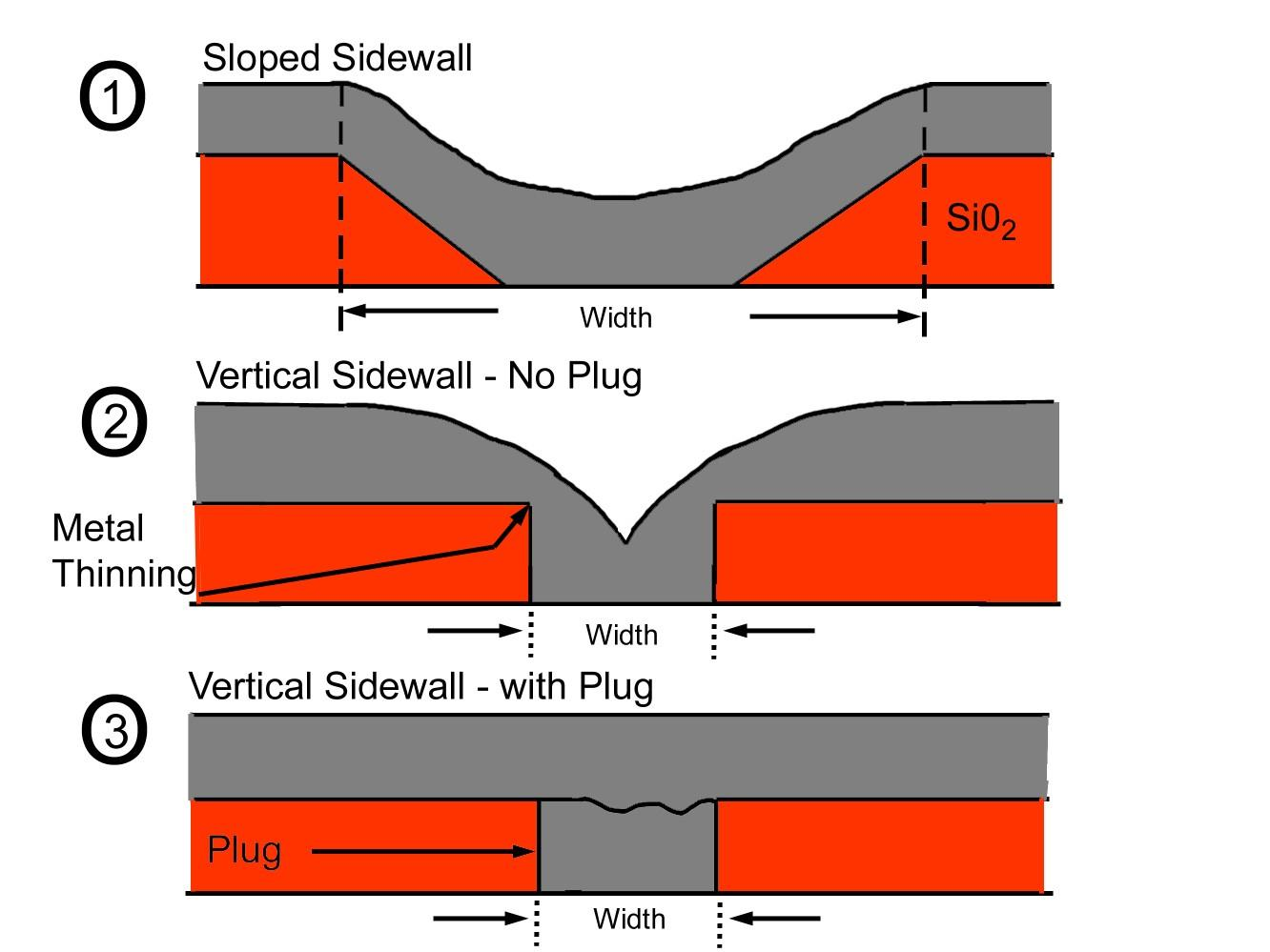
- Planar topography helps to prevents the metal thinning over steps 平坦化拓扑有助于防止金属在阶梯结构上的变薄
- Planarized Surface with vertical Plug fill prevents metal step coverage problem
经过平坦化的表面结合vertical Plug fill,可避免金属阶梯覆盖问题
- reduces line resistance 进而降低线阻
- Improve electromigration performance 改善电迁移性能
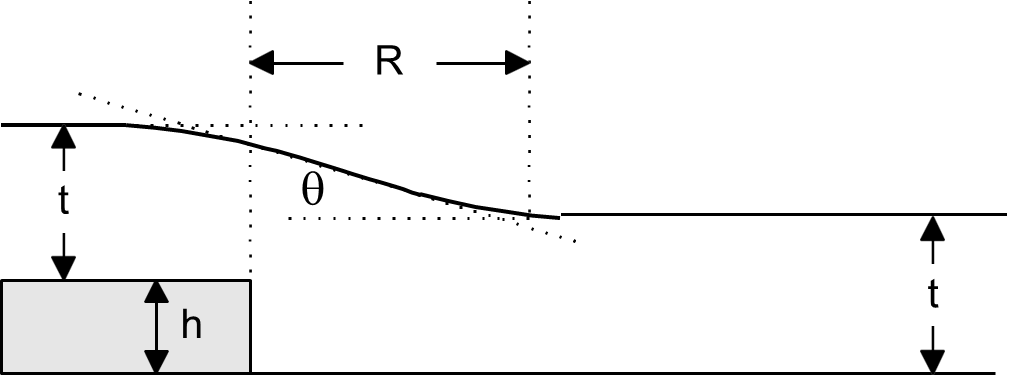
Quantitative Definition of Planarization
-
= the relaxation distance, (also called Planarization Distance PD) -
= planarization angle. -
Global Planarization:
- R > 10mm
-
achievable with Chemical Mechanical Polish (CMP)
CMP Basics
-
CMP is a physical-chemical process used to make wafer surfaces locally and globally flat. 化学机械抛光(CMP)是一种物理-化学过程,用于使晶圆表面在局部和整体上达到平坦化。
-
Chemical action
- hydroxyl (OH) ions attack SiO2 in oxide CMP, causing surface softening and chemical dissolution羟基(OH)离子在氧化物 CMP 过程中攻击 SiO₂,使表面软化并发生化学溶解
- oxidants enhance metal dissolution and control passivation in metal CMP 氧化剂在金属 CMP 过程中增强金属溶解,并控制钝化过程
-
Mechanical action
- polisher rotation and pressure 抛光机的旋转与压力
-
Why do we need CMP?
- for precise photolithography for advanced devices 用于先进器件的精确光刻工艺
- for advanced multilevel metallization processes 用于先进的多层金属化工艺
-
How is CMP evaluated?
- key parameter: post-polish nonuniformity (NU)
关键参数:抛光后非均匀性(NU)
- NU = ratio of the standard deviation of the post-polish wafer/film thickness to the average post-polish wafer/film thickness 抛光后晶圆/薄膜厚度标准差与平均抛光后晶圆/薄膜厚度的比值
- caused by variations in local removal rate 由局部去除速率的变化引起
- important parameter is removal rate (RR)
重要参数:去除速率(RR)
- RR = average thickness change during polishing divided by polishing time 抛光过程中平均厚度变化除以抛光时间
- key parameter: post-polish nonuniformity (NU)
关键参数:抛光后非均匀性(NU)
-
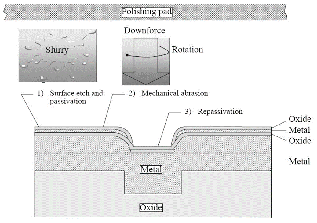
How does CMP work?
- A rotating wafer is pressed face-down against a rotating polishing pad; an aqueous suspension of abrasive (slurry) is pressed against the face of the wafer by the pad. 旋转的晶圆正面朝下压在旋转的抛光垫上;含有研磨颗粒的水基悬浮液(抛光液)通过抛光垫施加到晶圆表面
- A combination of chemical and physical effects removes features from the wafer surface.
- If mechanical only → scratches 产生划痕
- If chemical only → same as wet etching 作用类似于湿法蚀刻
![[Pasted image 20250425194121.png#pic_75center|]]
- Backing (or carrier) film provides elasticity between carrier and wafer
载体与晶圆之间是有弹性的Backing (Carrier) 膜
Carrier带着晶圆研磨
- Polishing pad made of polyurethane, with 1 mm perforations – rough surface to hold slurry 抛光垫由聚氨酯制成,带有 1 毫米的微孔——粗糙表面用于保持抛光液
- Wafer is polished using a slurry containing
- silica abrasives (10-90 nm particle size) 二氧化硅研磨颗粒(粒径 10-90 nm)
- etching agents (e.g. hydroxide for oxide,
for Cu to control pH) 蚀刻剂(例如用于氧化层的氢氧化物、用于铜的硫酸 ,以控制 pH 值)
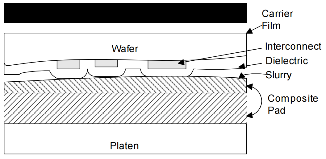
- Polymer polishing pad is pressed against the wafer surface. 聚合物抛光垫被压在晶圆表面
- Pad serves to transport the slurry to the wafer and provide pressure. 抛光垫用于将抛光液输送至晶圆,同时提供压力
- Both pad and wafer rotate in opposite directions. 抛光垫和晶圆沿相反方向旋转
- Over time, the pad becomes worn and must be reconditioned (scrubbed) with pad conditioner or replaced. 随着时间推移,抛光垫会磨损,需使用抛光垫调节器进行再处理(清洗)或更换
- The pad is an expensive consumable in the CMP process. 抛光垫是化学机械抛光(CMP)过程中昂贵的消耗品
CMP Equipment
CMP Polishing Pad 抛光垫
![[Pasted image 20250425194716.png#pic_75center|]]
- 表面多孔
- 用于填充抛光液
- 聚氨酯
- 坚韧的聚合物,硬度 = 55
- 纤维桩
- 比重 = 0.3
- 可压缩性 = 16%
- 均方根粗糙度 = 30μm
- 垫片机械模型 - 平面垫片
- 不考虑垫片微观结构
CMP Tool with Multiple Wafer Carriers
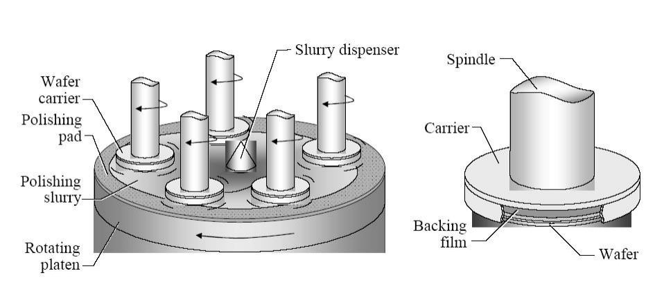
- 用对称排列的Carrier来提高抛光效率
CMP Slurry
- Chemicals in the slurry react with surface materials, form chemical compounds that can be removed by abrasive particles. 抛光液中的化学成分与表面材料反应,形成可被研磨颗粒去除的化合物
- Particulate in slurry mechanically abrade the wafer surface and remove materials.continuously flows between the wafer and the pad
抛光液中的微粒通过机械方式研磨晶圆表面并去除材料,同时在晶圆和抛光垫之间持续流动
- pad never actually touches the wafer 抛光垫永远不会直接接触晶圆
- slurry for polishing oxide films is alkaline (pH = 10 - 11) 用于抛光氧化膜的抛光液呈碱性(pH = 10 - 11)
- slurry for polishing metal films is acidic (pH = 0.5 - 4) 用于抛光金属膜的抛光液呈酸性(pH = 0.5 - 4)
- Chemical action of slurry changes top monolayers of film into soft material that is easily removed by motion of abrasive particles.
抛光液的化学作用使薄膜的表层单分子层转变为柔软材料,可通过研磨颗粒的运动轻松去除
- oxide film surface is hydrated 氧化膜表面发生水合反应
- metal film surface is oxidized 金属膜表面发生氧化反应
CMP Oxide Mechanism
![[Pasted image 20250425200933.png#pic_75center|]]
- 碱性溶液会把
变成 ,然后被抛光走
CMP Metal Mechanism
- Continuous oxidation, etching of the “high” metal surface results in planarization mechanism of CMP 持续氧化和蚀刻较高的金属表面,从而让表面平整
Characteristics of CMP Processes
-
Removal rate: microns/minute (typically 1-3)
- Requires pre- and post- film thickness readings, or In situ thickness measurements
(simple Preston’s Law), where: is removal rate is a constant for the specific process and equipment (function of film hardness, Young’s modulus,) is the pad pressure on the wafer surface is the relative velocity of the wafer and pad
- Typically, there is a tradeoff between removal rate (throughput) and an optimized process.
- Requires pre- and post- film thickness readings, or In situ thickness measurements
-
Uniformity of film removed or film remaining
-
Selectivity: (Removal rate of top film)/(Removal rate of lower film) - similar to etch selectivity
-
Defects:
- Particles
- Micro-scratches
- Residual slurry
![[Pasted image 20250425202647.png#pic_50center|]]
- Step Height Ratio:
- SHR is the ratio between
and SH_pre. is the difference between the max and min step height before the polishing, while is the step height difference after the polishing. 是 与 的比值。其中, 是抛光前最大和最小Step Height之间的差值,而 是抛光后Step Height的差值。 - Due to the polishing,
is always smaller than 1, and smaller means better planarity. 由于抛光作用, 始终小于1,且较小的 表示更好的平面度。
- SHR is the ratio between
Polish Termination During CMP
- Timed polish: Requires accurate polish rate, good uniformity, and is very monitor-intensive. 需要精确的抛光速率、良好的均匀性,并且对监控要求极高。
- Motor Current Endpoint: ?
- In-Situ Film Measurement: A built-in interferometer measures remaining film thickness through a window in the pad. Complicated by the presence of slurry and topographical features on the wafer surface. 内置干涉仪通过垫片上的窗口测量剩余薄膜厚度,但受浆料和晶圆表面的拓扑结构影响,使测量更加复杂。
CMP Process Concerns
Residual Slurry
- Slurry particles can be very difficult to remove, especially if they become trapped in deep holes or trenches. 浆料颗粒可能非常难以清除,尤其是在它们被困在深孔或沟槽中时。
- Soft rotating brushes in conjunction with
chemistry are used to mechanically remove residual slurry from both the wafer frontside and backside. 使用柔软的旋转刷子结合 化学处理,可在机械作用下去除晶圆正面和背面的残留浆料。
CMP Process Variables
- Mechanical (Tool)
- Pressure (down force) on the wafer
- Pad and wafer speeds
- Platen temperature
- Pad structure and conditions (ageing)
- Chemical Slurry
- Slurry flow rate (150-300 ml/min)
- Slurry chemistry
- Temperature
- Slurry age
- Pad Structure and Conditioning (ageing)
Process Issues
Effect of Structure Size & Density on Post Step Height
![[Pasted image 20250425205532.png#pic_75center|]]
- SHR is greater on metal pads compared to isolated narrow lines 相较于孤立的窄线,金属Pad上的SHR更高
- Areas with lower circuit density polish faster than areas with dense underlying topography 低电路密度区域的抛光速度比具有高密度底层拓扑结构的区域更快
- Each circuit design will have a different with-in die non-uniformity (WIDNU) due to variations in size and density of interconnects 由于互连尺寸和密度的变化,每种电路设计都会有不同的芯片内不均匀性(WIDNU)
Effect of Downforce on Removal Rate & Planarity
![[Pasted image 20250425205746.png#pic_75center|]]
- Increase in downforce (wafer pressure applied to the polishing pad) results in a linear increase in removal rate 下压力(施加在抛光垫上的晶圆压力)增加会导致去除率线性提升。
- Increase in downforce degrades planarity due to pad deformation and subsequent increase in local pressure at the ‘valley’ regions 由于抛光垫的变形以及随后在“谷底”区域局部压力的增加,下压力的增加会降低平坦度。
Effect of Platen Speed on Removal Rate & Planarity
![[Pasted image 20250425205850.png#pic_75center|]]
- Increase in platen speed increases removal rate linearly 旋转平台速度的增加会线性提高去除率
- Increase in platen speed improves planarity 旋转平台速度的增加有助于改善平坦度
- At higher speeds the pad contacts mainly the ‘hill’ regions since it does not have sufficient time to conform to the ‘valley’ regions 在更高的速度下,抛光垫主要接触“凸起”区域,因为它没有足够的时间适应“凹陷”区域
Effect of Carrier Speed on Wafer Center & Edge Removal Rates
![[Pasted image 20250425210023.png#pic_75center|]]
- Platen speed is maintained at 70RPM 旋转平台速度保持在 70RPM
- Center-to-edge removal rate difference increases with increasing carrier speed 随着Carrier速度的增加,中心到边缘的去除率差异也会增加
- Carrier diameter << platen diameter & at low carrier speeds, the linear velocity vector created by the carrier is much smaller than that created by the platen 载体直径远小于旋转平台直径,且在较低的载体速度下,载体产生的线速度矢量远小于旋转平台产生的线速度矢量
- As carrier speeds approach & exceed platen speed, the linear velocity vector created by the carrier becomes significant 当载体速度接近或超过旋转平台速度时,载体产生的线速度矢量变得显著
Effect of Pad Hardness on Post Step Height and Planarization Distance
![[Pasted image 20250425210153.png#pic_75center|]]
- Harder pads deform less under pressure thus leading to:
硬质抛光垫在压力下的变形较小,因此导致:
- Lower SHR, higher PD, and improved WIDNU (i.e in mm range) 更低的SHR、更高的PD,以及改进的芯片内不均匀性(WIDNU,毫米范围)。
- Poorer with-in wafer non-uniformity WIWNU (i.e. in cm range) 较差的晶圆内不均匀性(WIWNU,厘米范围)
- Harder pads also result in higher removal rates and higher defect densities 硬质抛光垫还会导致更高的去除率和更高的缺陷密度
Summary
| Parameter | Planarization Results on Wafer |
|---|---|
| Polish time | Amount of material removed |
| Pressure on wafer carrier (downforce) | Removal rate Planarization and non-uniformity |
| Carrier speed | Non-uniformity |
| Slurry chemistry | Material selectivity Removal rate |
| Slurry flow rate | Affects ow much slurry is on the pad and the lubrication properties of the system |
| Pad conditioning | Removal rate Non-uniformity Stability of CMP process |
| Wafer/slurry temperature | Removal rate |
| Wafer back pressure | Center slowness/non-uniformity Wafer breakage |
| 参数 | 晶圆上的平坦化结果 |
|---|---|
| 抛光时间 | 去除的材料量 |
| Carrier上的压力(下压力) | 去除率 平坦化和不均匀性 |
| Carrier速度 | 不均匀性 |
| 研磨剂化学成分 | 材料选择性 去除率 |
| 研磨剂流速 | 影响抛光垫上的浆料量及系统的润滑特性 |
| 抛光垫调节 | 去除率 不均匀性 CMP工艺的稳定性 |
| 晶圆/浆料温度 | 去除率 |
| 晶圆背压 | 中心区域抛光减缓/不均匀性 晶圆破裂 |
Post CMP Cleaning
-
Remove particles and chemical contamination following polishing 在抛光后去除颗粒和化学污染
-
Involves buff, brush clean, megasonic clean, spin-rinse dry steps 包括缓冲抛光、刷洗清洁、超声清洁、旋转漂洗烘干等步骤
-
Buffing
- after main polish , wafers “polished” using soft pads 主抛光之后,使用软垫对晶圆进行“抛光”。
- used following metal CMP 用于金属CMP后处理
- oxide slurries, DI water, or
used 采用氧化性研磨剂、去离子水(DI水)或 - changes pH of system to reduce adhesion of metal particles 通过改变系统pH值减少金属颗粒的粘附
- removes metal particles embedded in wafers 去除嵌入晶圆中的金属颗粒
- can reduce cleaning loads 可减少后续清洁负担
-
Brush cleaning
- brushes made from PVA with 90% porosity 刷子由聚乙烯醇(PVA)制成,孔隙率达90%
- usually double sided scrubbing, roller or disk-type 通常采用双面擦洗方式,可为滚筒式或盘式
- brushes probably make direct contact with wafer 刷子可能直接接触晶圆表面
(1-2%) added for particle removal (prevents redeposition), citric acid (0.5%) added for metal removal, HF etches oxide to remove subsurface defects 添加 (1-2%) 以去除颗粒(防止颗粒重新沉积),添加柠檬酸 (0.5%)以去除金属,HF 用于蚀刻氧化物以去除表面下缺陷
-
Megasonic cleaning
- sound waves add energy to particles, thin boundary layers 声波为颗粒提供能量,减薄边界层
- cleaning chemicals added (SC1, etc.) 添加清洁化学品(SC1等)
- “acoustic streaming” induces flow over particles “声学流动”(Acoustic Streaming)诱导流体在颗粒表面流动,以辅助清洁
-
Spin-rinse drying
- following cleaning, wafers rotated at high speed 清洁后,晶圆以高速旋转
- water and/or cleaning solution (SC1) sprayed on wafer at start 在初始阶段喷洒水或清洁溶液(SC1)
- hydrodynamics drain solutions from wafer 通过流体动力学作用排出晶圆上的溶液
- probably no effect on cleaning, but ensures that particles dislodged from wafer during preceding steps do not resettle on wafer 可能不会直接影响清洁效果,但确保前面步骤中脱离晶圆的颗粒不会重新沉积回晶圆表面
Advantage
| Benefits | Remarks |
|---|---|
| Planarization | Achieves global planarization |
| Planarize different materials | Wide range of wafer surfaces can be planarized |
| Planarize multimaterial surfaces | Useful for planarizing multiple materials during the same polish step |
| Reduce severe topography | Reduces topography to allow for fabrication with tighter design rules and additional interconnection levels |
| Alternative method of metal patterning | Provides an alternate means of patterning metal (e.g., Damascene process), eliminating the need of the plasma etching for difficult-to-etch metals and alloys |
| Improved metal step coverage | Improves metal step coverage dueto reduction in topography |
| Increased IC reliability | Contributes to increasing IC reliability, speed and yield (low defect density) of sub- |
| Reduce defects | CMP is a subtractive process and can remove surface defects |
| No hazrdous gases | Does not use hazardous gases common in dry etch process |
| 优势 | 备注 |
|---|---|
| 磨平 | 实现整体平整 |
| 磨平不同材料 | 可对多种晶圆表面进行磨平 |
| 磨平多种材料表面 | 在同一个抛光步骤中磨平多种材料具有重要作用 |
| 减少严重的拓扑结构 | 降低拓扑复杂度,以适应更严格的设计规则并支持额外的互连层 |
| 金属图案化的替代方法 | 提供一种金属图案化的替代方法(如大马士革工艺),避免对难以蚀刻的金属和合金进行等离子蚀刻 |
| 改善金属阶梯覆盖 | 由于拓扑结构的减少,可提升金属阶梯覆盖质量 |
| 提高集成电路(IC)可靠性 | 有助于提升亚 |
| 减少缺陷 | CMP是一种减材工艺,可用于去除表面缺陷 |
| 无有害气体 | 不使用干法蚀刻工艺中常见的有害气体 |
Disadvantage
| Disadvantage | Remarks |
|---|---|
| New technology | CMP is a new technology for wafer planarization. There is relatively poor control over the process variables with a narrow process latitude. |
| New defects | New types of defects from CMP can affect die yield. These defects become more critical for sub- |
| Need for additional process development | CMP requires additional process development for process control and metrology. An example is the endpoint of CMP is difficult to control for a desired thickness. |
| Cost of ownership is high | CMP is expensive to operate because of costly equipment and consumables. CMP process materials require high maintenance and frequent replacement of chemicals and parts. |
| 缺点 | 备注 |
|---|---|
| 新技术 | CMP是一项用于晶圆平坦化的新技术。对工艺变量的控制能力较弱,且工艺范围较窄 |
| 新缺陷 | CMP可能会产生新的缺陷,影响芯片良率。对于亚 |
| 需要开发额外的工艺 | CMP需要开发额外的工艺,以实现工艺控制和计量。例如,CMP的终点控制较难,难以精确控制所需的厚度 |
| 拥有成本高 | CMP的运营成本较高,因为设备和耗材昂贵。CMP工艺材料需要高频率维护,并且化学品和零部件需要经常更换 |