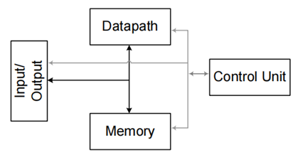
Generic Digital System
A Generic Digital System consists of:
- Datapath
- Control Unit
- Memory
- Input Output Modules
Arithmetic Modules
- Datapath in digital systems consists of mainly arithmetic modules
- Common arithmetic modules include Adders (Subtractor), Multipliers, Shifters
Power Considerations in Datapath
-
To compensate the reduction of speed, design techniques can be used 为了弥补速度的下降,这些技术被使用了:
- Parallel functional blocks operate at lower frequency and lower
can be used to process data in parallel to compensate loss of performance 较低频率和较低 下运行并行功能模块,可以并行处理数据以补偿性能损失 - Pipeline structure of functional blocks can also be used to save power as lower
is needed to charge smaller capacitance for the same speed 功能模块的流水线结构也可以节省功率,因为相同速度下需要较低 来充电较小的电容。
- Parallel functional blocks operate at lower frequency and lower
Clock Gating
Power Gating
Other Low Power Techniques
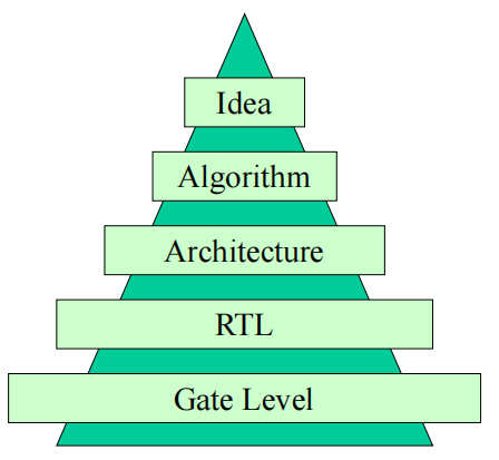
Design Methodology
Design Complexity
Intel Microprocessors
看图(铸币大头凑近)
Moore’s Law
- Gordon Moore:
- Fairchild Corporation
- Cofounder of Intel
- Prediction in 1965: “The number of transistors incorporated in a chip will approximately double every 24 months.”
Design Abstraction Levels
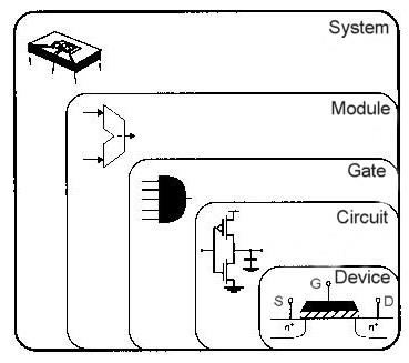
Gajski-Kuhn Y Diagram
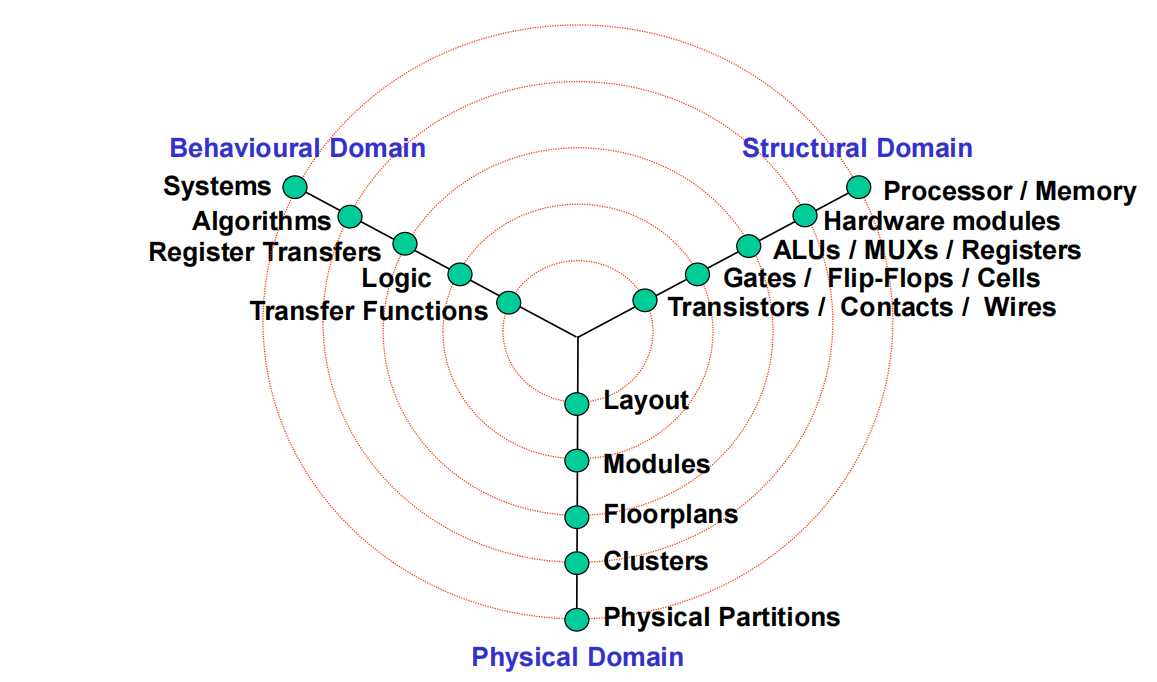
Objects In Each Domain
| Behavioural | Structural | Physical | |
|---|---|---|---|
| System | Performance Specs. | CUPs Memories Controllers Buses | Physical Partitions |
| Algorithmic | Data Procedures | Hardware Modules Data Structures | Clusters |
| Microarchitectural | Operations Register Transfers State Sequencing | ALUs MUXs Registers Microsequencer | Floorplans |
| Logic | Boolean Equations FSM | Gates Flip-Flops Cells | Cell / Moudle Plans |
| Circuit | Transfer Functions Timing | Transistors Wires Contacts | Layout |
Design Hierarchy
Design Flow
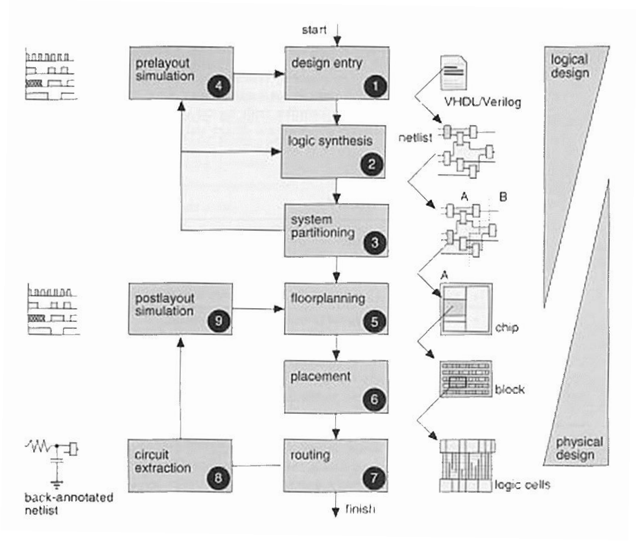
Design Entry
- Text based Hardware Description Languages
- VHDL
- Verilog
- Schematics
- State Diagram
- Flow Chart
Synthesis, Partitioning & Simulation
- Logic Synthesis
- Use synthesis tools to translate HDL to a netlist of logic gates and their connections
- System Partitioning
- Divide a large system into smaller blocks
- Several ICs if necessary
- Prelayout Simulation
- Verify the functionality of the system
Floorplanning, Placement & Routing
- Floorplanning
- Arrange the blocks of the design to optimize the size and the interconnections
- Placement
- Decide the locations of modules and logic cells
- Routing
- Make connection between cells and modules
Extraction & Postlayout Simulation
- Extraction
- Convert the layout back to circuits
- Determine the resistance and capacitance of the interconnect
- Postlayout Simulation
- Verify the functionality again, with the added loads of the interconnect
- Verify the timing
EDA Tools
4 Main Categories: