- In a FET there is a gate-controlled channel through which current is allowed to flow. 场效应管中有一个受到栅极控制的沟道,电流能够在其中流动
- The gate must be isolated from the channel current flow. Otherwise, an input signal current, while on its way to the output, would “leak” through the gate, leading to a poor gain for the FET. 栅极必须与沟道电流隔离。否则,输入信号电流在到达输出时会“泄漏”到栅极,导致FET增益变差。
Two types of conventional FETs

- Metal Oxide Semiconductor FETs (MOSFETs)
金属氧化物场效应管
- The gate isolation is provided by depositing an oxide between the gate and the active channel. 栅极使用在栅极与有源沟道之间的氧化物绝缘
- The n-channel is induced at the p-type
surface due to strong inversion associated with band bending and controlled by gate voltage . 在p型衬底表面的n型沟道在强反型的作用下会发生能带弯曲,受到 的控制 - The electron flow in the channel forms current
when , and . 当 、 时,电子流过沟道形成

- Metal Semiconductor FETs (MESFETs)
金属半导体场效应管
- In a Metal Semiconductor FET (no oxide), the metal gate forms a Schottky Barrier with the semiconductor. 在MESFET中(没有氧化物),金属栅极与半导体形成了肖特基势垒
- The n-channel is a part of the n-type Si, which is not covered by the depletion region of the Schottky Barrier, and controlled by the reverse-biased Shottky contact. n型沟道是n型衬底的一部分,不与肖特基势垒的空间电荷区重合,受到反偏肖特基接触的控制。
New FETs Developed Using Heterostructures
- Modulation-doped Field Effect Transistors (MODFETs)
- They are also called:
- Heterostructure Insulated Gate FETs (HIGFETs)
- High Electron Mobility Transistors (HEMTs)
- Two-dimensional Electron Gas FETs (TEGFETs)
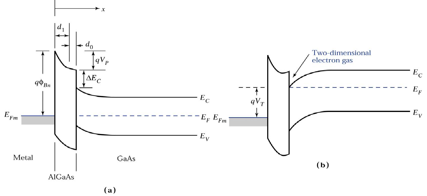
Device Structures

- Semi-Insulating GaAs Substrate. 半绝缘GaAs
- Undoped GaAs, 2-dimensional
gas is formed on the surface of this layer. 未掺杂的GaAs,这个区域会形成二维电子气 - Undoped AlGaAs as a spacer which separates the electrons in undoped GaAs and the donor ions in doped AlGaAs. 未掺杂的AlGaAs形成间隔层,将未掺杂GaAs层的电子和掺杂的AlGaAs层的施主离子隔离
- Donor-doped AlGaAs. 施主掺杂的AlGaAs
- Metal gate which forms Schottky Barrier with the doped AlGaAs. 金属栅极,与掺杂的AlGaAs形成肖特基势垒
The energy band profile shows band bending leading to a triangular quantum well at the
![[MODFET_FIG4.png#pic_center|]]
Modulation Doping
![[MODFET_FIG5.png#pic_center|]] ![[MODFET_FIG6.png#pic_center|]]
- The doped wide bandgap
AlGaAs has donor ions and electrons. 宽带隙的 AlGaAs有施主离子和电子 - The electrons could transfer through the undoped AlGaAs spacer to the narrow bandgap undoped GaAs as it has lower energy states for electrons. 电子穿过未掺杂的AlGaAs隔离层到窄带隙的GaAs,因为GaAs层的电子能级更小
- The positively charged donor ions and the negatively charged electrons are then spatially separated by the undoped AlGaAs spacer. 正电荷施主离子和负电荷电子被未掺杂的AlGaAs层上在空间上分开
- The dipole effect produces band bending. 偶极效应导致能带弯曲
- The energy states in undoped GaAs are quantized,
is the ground level. 未掺杂GaAs中能级是量子化的, 是基态
Advantages of the Modulation Doping
- Because the electrons at the surface of the narrow gap GaAs are spatially separated from the positively charged dopant ions by the undoped AlGaAs spacer, these electrons are virtually free to move in the undoped GaAs channel and essentially remain free from impurity ion scattering. Thus, they have high mobility.
由于在窄带隙GaAs表面的电子从空间上与带正电的杂质离子被未掺杂的AlGaAs隔离层隔离,这些电子在未掺杂的GaAs沟道中几乎可以自由移动,并且基本上不受杂质离子散射的影响。因此,它们具有高迁移率。

- As the trapped electrons have 2-dimensional properties (moving in x-y plane), hence they are called two-dimensional electron gas. The sheet electron concentration is very high as they are limited to a very thin surface layer of the GaAs. 由于被捕获的电子具有二维特性(在x-y平面内移动),因此它们被称为二维电子气。面电子浓度非常高,因为它们被限制在非常薄的GaAs的表面层。
![[MODFET_FIG8.png#pic_center|]]
- The two-dimensional electron gas has the highest Carrier Mobility at a given temperature. 这个二位电子气在给定的温度下有最高的迁移率
- This is why such devices are also called High Electron Mobility Transistors (HEMTs). 这就是为啥这货叫HEMT
Normally-off and normally-on Devices
- To control the drain-source current
by means of a gate voltage , the thickness of the wide bandgap layer between the gate metal and the 2DEG is critical. 为了使用栅极电压 控制漏-源电流 ,栅极金属和二位电子气之间宽带隙层的宽度非常关键 - By varying the thickness of the wide-bandgap layer, the MODFET can be made either a normally off (enhancement mode) or normally on (depletion mode) device. 通过修改宽带隙层的厚度,MODFET可以制作成常开或者常闭器件
Normally-off or Enhancement-mode MODFETs
- When the wide-bandgap layer is thin, the MODFET will be a normally-off device. 当宽带隙层比较薄的时候,MODFET是一个常开器件。
-
Energy band diagrams of a normally-off MODFET at 常开MODFET的能带图,条件:
- (a) Thermal Equilibrium 热平衡下
- (b) The onset of threshold (
) 达到阈值电压
-
and are the thicknesses of the doped and undoped regions of the wide bandgap semiconductor, respectively 和 分别是是掺杂和没掺杂的宽带隙层的厚度 -
is the conduction bandgap offset 是导带带隙的偏移 -
For small AlGaAs thickness, the gate Schottky Barrier can completely deplete the electrons in the AlGaAs as well as the 2DEG even at zero gate bias, thus leading to enhancement-mode type or normally off devices. AlGaAs厚度较小的情况下,即使没有栅极偏置,栅极的肖特基势垒也可以完全耗尽AlGaAs和二位电子气中的电子,从而获得了增强型或者常闭型器件。

The depletion width of the Schottky contact
is greater than . No channel is formed at the narrow bandgap GaAs surface. 肖特基接触的耗尽层宽度 ,在窄带隙的GaAs表面未形成沟道 -
A positive gate voltage (greater than the threshold voltage
) is required to turn the device on. When , the depletion width 大于阈值电压 的正栅极电压可以开启器件,当 时, ![[Pasted image 20241102024935.png#pic_center|]]
The threshold voltage can be adjusted by control of AlGaAs thickness and doping.
阈值电压可以通过调整AlGaAs的厚度和掺杂实现
- When the gate voltage is larger than
, a charge sheet will be capacitively induced by the gate at the heterojunction interface. 当栅极电压大于阈值时,受到栅极的影响,异质结的界面上将出现一个电容性的电荷层 ![[Pasted image 20241102025701.png#pic_center|]]
The sheet carrier concentration (number of the carriers per unit area) is defined as
电荷层的载流子浓度被定义为:
is zero at the source and at the drain 在源极为0,在漏极为 (沟道的长度) is the voltage at position due to drain voltage 沿着 方向的漏极电压 is the deleption capacitance per unit area 单位面积的耗尽电容 Where is a correction factor (some authors take as the thickness of channel or inversion layer) 是一个矫正系数(一些作者把这个定义为沟道或反型层的厚度)
Normally-on or Depletion-mode MODFETs
-
When the wide bandgap layer is thick enough, the MODFETs will be Normally-on or Depletion-mode devices. 当宽带隙层足够厚,MODFET会变成常闭器件
-
For thicker AlGaAs layers, the depletion region of the Schottky Barrier does not deplete the electron gas at zero gate voltage (
). Such devices are Normally-on or Depletion-mode devices. (A channel exists at ). 对于更厚的AlGaAs层,在栅极电压为0的情况下,肖特基势垒并不会把二维电子气耗尽到0V( )。这种器件被称为常闭或者耗尽型器件( 时存在沟道) ![[Pasted image 20241102030333.png#pic_center|]]
-
A negative gate voltage is required to deplete the electron gas and pinch the device off. (
) 负的栅极电压用来耗尽二维电子气以将设备关闭 
Example
Consider an AlGaAs/GaAs heterojunction with n-AlGaAs doped to
Solution
- 首先判断器件类型(常开还是常闭),判断依据是阈值电压
- 肖特基势垒
- pinch-off voltage:
- 掺杂浓度
- AlGaAs厚度
- 相对介电常数
,所以介电常数为 所以阈值电压 :
- 掺杂浓度
- 肖特基势垒
- 二维电子气浓度
:
Current-Voltage Characteristics
- The current voltage characteristics of a MODFET can be obtained in the way similar to the MOSFET. The current at any point along the channel is
MODFET的电压电流特性可以用和MOSFET类似的方式获得,沟道任意一点的电流为:
Where: is the channel width 沟道宽度 is longitudinal electric field 沿着沟道的电场强度
- Since the current is constant along the channel, integrating the equation from source to drain (
to ) gives 因为这个电流在沟道中是一个常数,对这个等式从源到漏积分得到: - When
, it is in linear region and 当 ,它在线性区 - At large drain voltage, the charge sheet
at the drain is reduced to 0. So and the saturation current is 漏极电压比较大的时候,漏极的电荷层 被减小到0, 。所以饱和电流为: - For high-speed operations, the longitudinal field along the channel is sufficiently high to cause carrier drift velocity saturation (
). The current (maximum) in the velocity-saturation region is 对于高速应用,沿着沟道的电场非常大,导致载流子达到速度饱和。此时的最大电流为:
- When
Important Parameters
Channel Conductance
is Carrier Mobility 载流子迁移率 is electric field and , is channel length 电场强度
With
Transconductance
- 其中
是速度饱和的速度
Transit Time
MODFETs have very small transit time that enables them to be used as high-speed devices. MODFET有非常小的传输时间,适用于高速设备
Cutoff Frequency
- The speed of a MODFET is measured by the cutoff frequency
MODFET的速度使用截止频率衡量
where: is the parasitic capacitance 寄生电容
- To improve
, we should consider a semiconductor with large , a gate structure with an ultra short gate length, and a device configuration with minimum parasitic capacitance. 为了提高截止频率,我们要考虑一个有大速度饱和速度的器件,栅极极其短的栅极结构,设备结构上的寄生电容尽可能小
Cutoff Frequency Versus Channel or Gate Length for Five Kinds of Field-Effect Transistors

- The best pseudomorphic SiGe MODFETs have a
comparable to the GaAs MODFET. SiGe MODFETs are attractive because they can be processed with silicon fabrication facilities. 最好的伪SiGe MODFET的截止频率与GaAs MODFET相当,SiGe MODFET相当有吸引力,因为它可以用硅的制造设备制造。 - The
MODFET formed on a InP substrate has higher , mainly due to the high electron mobility and velocities in the . The at a gate length of can be as high as .
Summary
- The MODFET is a device which enhanced high-frequency performance. This device structure is similar to that of a MESFET except there is a heterojunction under the gate. A two-dimensional electron gas, i.e., a conductive channel, is formed at the heterojunction interface, and electrons with high mobility and high average drift velocity can be transported from the source through the channel to the drain. MODFET是一种增强高频性能的器件。其结构类似于MESFET,但在栅极下方有异质结。在异质结界面形成了二维电子气,即导电沟道,具有高迁移率和高平均漂移速度的电子可以从源极通过沟道到达漏极。
- The output characteristics of all field-effect transistors (FETs) are similar. They all have a linear region at low-drain biases. As the bias increases, the output current eventually saturates, and at a sufficiently high voltage, avalanche breakdown occurs at the drain. Depending on whether it requires a positive- or negative-threshold voltage, FET can be either normally off (enhancement mode) or normally on (depletion mode). 所有场效应晶体管(FET)的输出特性都相似。它们在低漏极偏置时都有一个线性区域。随着偏置的增加,输出电流最终会饱和,并且在足够高的电压下,会在漏极处发生雪崩击穿。根据是否需要正阈值电压或负阈值电压,FET可以是常断型(增强模式)或常通型(耗尽模式)。
- The cutoff frequency
is a figure of merit for the high-frequency performance of a FET. The conventional GaAs MODFET and the pseudomorphic SiGe MODFET have a about 30% higher than that of the GaAs MESFET. The GaInAs MODFET has the highest and it has a projected of at a gate length of . 截止频率 是评估 FET 高频性能的指标。传统的 GaAs MODFET 和伪SiGe MODFET 的 大约比GaAs MESFET高30%.GaInAs MODFET具有最高的 ,在 栅极长度下的 为 。