Q1
- The short channel effect in MOSFETs refers to the phenomenon, lowering of
etc. , happens when the length of gate shrink to close to the width of depletion layer . - When the MOSFET is under SCE, the drain current will increase with the drain-source voltage due to Channel Length Modulation Effect; The subthreshold swing will increase which makes the device hard to close completely; The threshold voltage could decrease due to Drain Induced Barrier Lowering.
- According to the formula
, there could be at least three ways to suppress the SCE, - Increase the
by using high-k material or reducing the thickness of oxide; - Increase the
to decrease the to minimize the chance of punchthrough (Channel Engineering); - Decrease the junction depth
by using the shallow junction;
- Increase the
Q2
Reasons why MOSFET made on Si has better high frequency performance are listed as follow,
- Scaling down has improved the transconductance and decrease the gate capacitance, which made the progress in cutoff frequency of Si MOSFET;
- Introducing tensile strain and compressive strain through strained silicon technology to improve carrier mobility;
- Using of high-k dielectric and metal gate optimizes gate capacitance and transconductance
- Fin-FET and GAA-FET enhanced the control ability of gates;
- Shallow junction and Salicide decrease the source/drain resistor.
Q3
Tensile strain will change the shape of energe band, the lift of the CB degeneracy will reduce the intervalley scattering results in mobility improvement. Thus the cutoff frequency
Q4
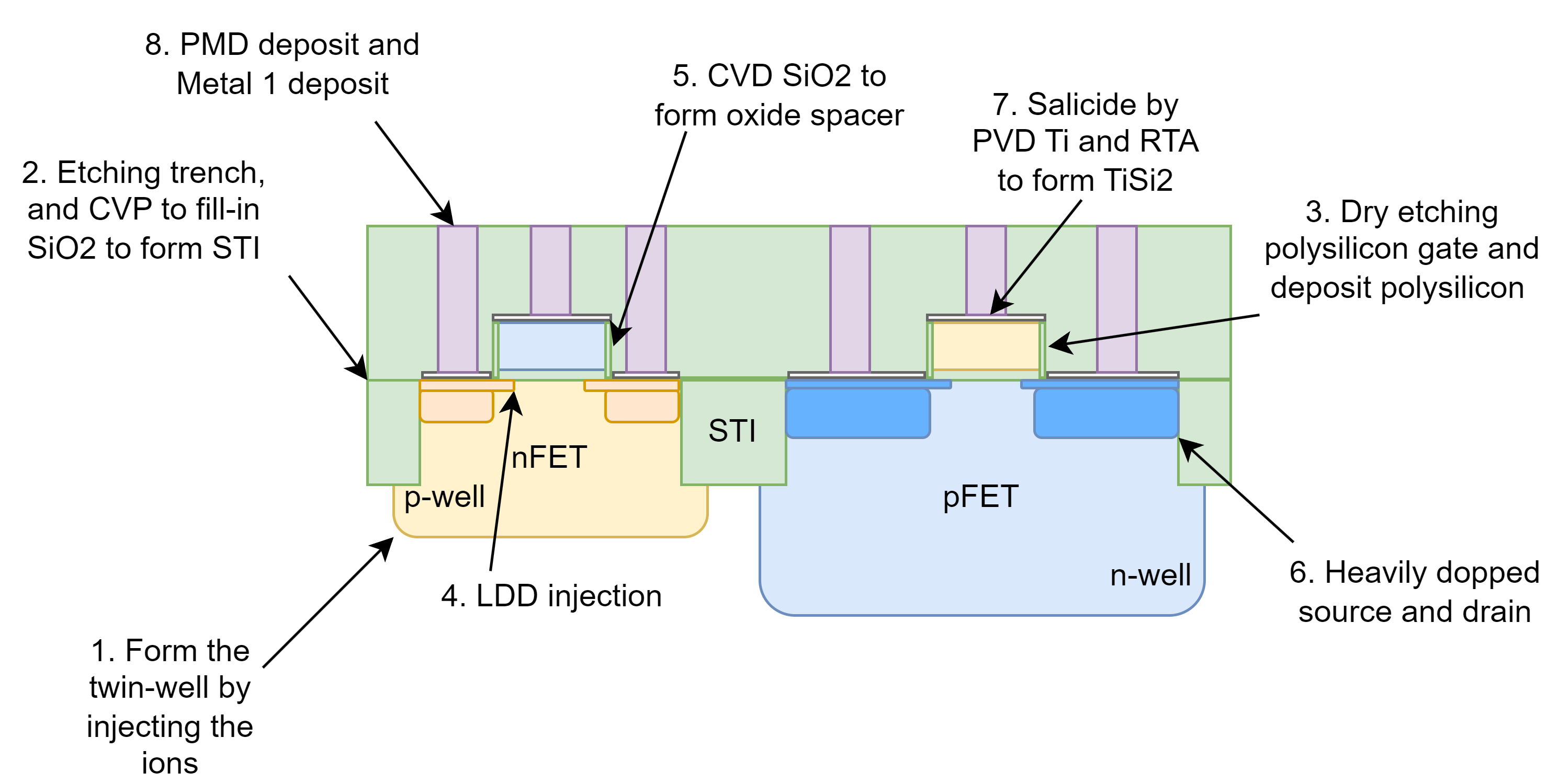
The FEOL CMOS fabrication flow can be described as follow,
- Using p-type silicon substrate, photolithography defines the N-well and P-well, i mplants phosphorus and boron saperately;
- Dry etching forms a shallow trench, filling with
; - Deposition of high-k dielectrics to form the gate;
- Source and drain extension injection to form a shallow junction;
- Formation of sidewall spacer;
- Source (drain) injection to form a doped region;
- Self-aligned silicide metal deposition;
- contact hole etching and PVD the Cu to form Metal 1 interconnectio
Q5
- By choosing the right metal, its thermal expansion coefficient can be made close to that of high-k dielectrics, thereby reducing thermal stress. Metals can also be integrated at low temperatures, avoiding high temperatures. As conductors, metals can also evenly distribute the electric field, reducing the risk of breakdown;
- Metal materials (such as TiN) are dense and have stable lattices, which block the migration of impurity atoms;
- The metal gate is a continuous thin film without polysilicon grain boundary defects, thus avoiding the oxidation of high-k dielectric to form a low-k interface layer.